Revisiting Electron Transport in Solid State Physics
If one is only interested in electron transport behavior in materials, it's usually sufficient to know a few things about the band structure, rather than the entire crystal structures. Without going into the geometry of crystal structures in 3 dimensions (which could be something for another time) there are 14 ways that atoms can be arranged in a 3-dimensional crystal structure. That gives rise to the 14 Bravais lattices that exist. This, until we figure out how to touch time-crystals, is the highest level of complexity that the problem can take on, so in theory we know about the most complex a band structure can become. Still, it usually suffices to take a glance at the band structure of a 1D crystal.
I'll presuppose the basics of quantum mechanics at this point, and if they happen not to be present, I'd like to point the reader towards the run-down of quantum physics in the Deep Dive series. Suffice it to say that for an electron traveling along a one-dimensional crystal, the energy potential is like that of equidistant barriers, which will form a series of identical potential wells. Within potential wells, the energy of free electrons follows the parabola-shape of the harmonic oscillator with the signature quantized steps between energy levels.

When electrons travels along the crystal structure, every barrier will reflect a certain percentage of electrons, while transmitting the remaining ones. At the energy levels, one will be able to find resonance energies at which electrons can transition between energy levels. In a weak potential, the different levels can be approximated by a series of parabola shapes, with the extrema resting on the level divide. Upon closer inspection, the curves will tend asymptotically towards the next energy level from below, which is necessary for the transfer to be even possible, but it'll produce a somewhat odd-looking curve, that will actually have some (infinitesimal) gaps. Since the crystal structure is periodic and depends on both the height and width of the potential barrier, it makes sense to introduce a periodicity to the potential as the electron moves along the structure. Trivially, we can assume that V(x) = V(x+a) where a is the lattice constant. This is the potential that one would apply to the Schroedinger Equation. The solution to this is easily found using the plane-wave ansatz, so it takes the form Ψ = exp(±iKx)u(x) where u(x) is some function periodic with the lattice constant, and often parametrized with the wave vector. By checking the periodicity of Ψ, one can find that Ψ(x + a) = exp(iKa)Ψ(x). This is known as "Bloch's Theorem". This introduces a periodicity into the band structure, which means that one only needs to know a relatively small part of the band structure along a crystal. Further, the most important portion of the band structure is really only the "band gap", which returns a certain form. The band gap diagram is a projection of the Brillouin Zone along certain characteristic vectors, which exists in reciprocal space anyway, making it an abstraction of a shape in a space that can never be directly observed either way. As such, usually little is gained by looking at the full diagram, so it's usually simplified down to the band gap minimum, which is approximated by two parabolas with an energy gap. The band with the higher energy is considered the "conduction band" and the one with the lower the "valence band", occasionally abstracted down to the edges, since really only the minimal gap matters. For two different materials, the adjacent band gaps can just be charted next to one another, as we approximate that the lattice constant is vanishingly small in comparison to any two pieces of adjacent matter. This bandgap also has some effect on the optical properties of the material, becoming more optically dense with smaller gap energies. It also carries and effect on the effective mass of the material, which is here defined as a tensor, meaning it has dependencies in its direction. We're already aware that there is more than just one mass definition, which implies that there has to be more than just one band. The valence band is actually made up of several bands that touch at the curve maximum. There's a distinction made between the heavy and light hole mass. The way electrons are arranged around a nucleus will define this mass by the longitudinal and transversal curvature of the (statistical) electron clouds, which can give two electric masses. Such is the case for indirect semiconductors. Direct semiconductors have the same curvature for both directions. Note that the above, while defined for 1D-materials is not actually valid independent of dimensionality. It's so far been a discussion of 3D materials, since those are the most often encountered, and might then be seen as the most general. The 2D case is somewhat different, but does exist in the real world.
Conductability is only tangentially determined by the band gap. Much more important is the existence of empty (or unoccupied) states for electrons to move through. Of course the band gap will have to accommodate for states in the first place, but the second part of the consideration is the level to which they are filled. Often these empty states sit in the conduction band which has naturally higher energy, while the electrons sit in the valence band, but in these cases the electrons will have trouble jumping the energy gaps. For semiconductors, the conduction band is even partially filled, which means that electron transport becomes a lot easier along the k-direction. Of course we note that the hole itself is primarily defined by the electrons surrounding it. It's not a particle or intrinsic feature of a structure, so substituting it with a positron, for example, is not a viable move in a discussion. Getting partially filled conduction bands will entail leaving holes in the valence band, or the material will behave ionically, which wasn't really the point. Instead, the electrons will have to experience some excitation (usually either optical or thermal) that exceeds the energy gap. The electron will jump from it's "home" in the valence band to the conduction band and leave an electron hole. Electron transport from there will see the electrons moving in one direction. One could view this as the electron in the conduction band move in one direction, while the hole in the valence band moves in the opposite direction. Alternatively one could find a "dopant band" near the conduction band, which donates an electron. This way won't generate a hole. The same could be done by finding a dopant band to accept an electron from the valence band and generate a hole without the extra electron in the conduction band. These dopant bands usually enter the structure ionically and the electrons within it remain stationary. The former is called n-doping while the other is called p-doping.
We recall the Pauli exclusion principle from quantum mechanics. When observing systems of electrons, this principle implies that the potential energy of the system will change rather drastically, if some electrons are elevated above their "resting" state. Doing this is relatively trivial - introduction of thermal energy, meaning temperature, can excite electrons. Assume all electrons occupy the state of minimal energy. The highest possible energy an electron might adapt in this state is called the "Fermi Energy" and it depends only on the size of the electron ensemble, and the quantization of possible electron states. Any excitation will introduce a probability that the state of an electron is above the Fermi energy. This opens the door to a statistical function, called the "Fermi-Dirac Statistics" function, which gives the probability that an electron carries some energy E.

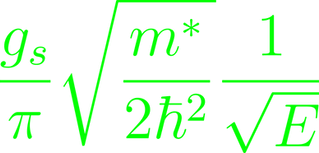
This also implies some non-trivial density of states depending on the energy D(E). There are established formulas for the development of D(E) in 1 - 3 dimensions, along with the Fermi-vector and the Fermi-energy. Most importantly for D(E) are the ways in which the effective mass and the energy factor into the equation (the rest are constants). Both scale up with a square root factor for each added dimension. For 1D, this becomes
Surprisingly, the 2D case has no energy dependency for the state density. To observe the change in the density of states for a temperature (stand in for statistical excitation), one can compute either of the following integrals

They are of course complementary.