Charge Transport in Materials
Production of Semiconductors
Semester's starting up again, and some courses come along with stuff I need to revise, so expect the Aerodynamics stuff to be liberally interspersed with other stuff for the next months. The course I'm visiting is mainly concerned with transport of charges, which, in reality, will usually take place in semi-conductors. These are rather complex structures, and their physical properties, namely the band-structure, will be determined much more by the layering of materials than any of the individual materials included. Such a structure, however, needs to grow on a sort of template, that will enable the correct layering in the first place. Because of that, they are grown onto a "wafer". The production of the wafer depends on the use case, or rather on how precise the band structure will need to be. Wafers are a type of crystal, so they need to be grown in production. This is either done through cultivating the crystal, so-called "bulk growth" or a more precise "epitaxial growth". The idea behind using a crystal as the base is that a crystal structure is naturally self-repeating and hence electrons traveling through the structure don't experience a lot of scattering. Little scattering (or statistically: long scattering times) mean the interaction effects are conserved over longer times. If they are weakened too much through scattering, some (usually quantum) effects can completely disappear. However, this is only true for so-called one-crystals. Bulk growth usually doesn't create one crystals, meaning that the epitaxy is the preferred method of creating the wafer.
The epitaxial growth process usually involves a seed crystal being dipped into a bath which facilitates crystal growth, then pulled out of the bath while spinning. For the layers that are grown on top of the wafer though, there are some geometric constraints for the material though. The lattice constant of the layers will determine the geometry of the layering. If the lattice constant of base and new layer are at least similar, then they'll stack directly on top of one another, but if they differ too much, the particles might clump in more or less random intervals. There are certain, slightly complicated ways to build clumps on top of a new layer (Stranski-Krastanow-Growth) which will still require similar lattice constants, which are used for many optical observations. And then there is the question of how to actually cultivate these new layers onto the wafer. In industry, where quantum effects aren't yet widely utilized, it suffices to use a chemical process, i.e. spilling a chemical mix onto a spinning wafer. The obvious problem here is of course the same possibility of lattice defects which reduce scattering time that influences the choice of wafer construction. The much more precise version of this is the MBE (molecular beam epitaxy) method, which sees heated vapor of exactly the molecules required for the formation of the material hitting the wafer, possibly with a dopant, if necessary. Often the substrate is heated up, to help the reaction along. This method is clearly more complicated to do, even before noticing that MBE needs a pressure of 10^-9 to 10^-12 mbar, compared to the 10^-3 to 10^-5 mbar in the MOCVD version. MBE is also significantly slower.
To fashion a semiconductor from a neat block of chemical layer-cake into the metallic and (usually) green pieces of electronics that populate most modern tools will require it undergo a lithography process to expose, or insulate the relevant portions. The photo-resist method has the chemical mix with a hardnened resist on a spinning wafer topped off by an optical mask, through which the structures are engraved using high-energy light. This last step is also called "illumination" often a UV light suffices for it. There's a distinction made between positive resist, which is destroyed under UV light, and the negative resist, which stabilizes under UV light by cross linking the polymer chains. Whether the resist is positive or negative will of course determine whether the mask is a positive or negative print. An alternative is etching, which often used by hobbyist on account on not necessarily requiring a lab. The distinction here is made between wet and dry etching, where wet etching is the chemical etching, which carries the risk of creating non-smooth edges by a phenomenon called "underetching". The other option is reactive ion etching, which is a bunch more expensive, since it involves shooting ions onto the spots where material is supposed to be removed. There is a possibility for the material to change by this process.
Semi-Classical Electron Transport & Quantum Effects in Nano-Structures
The way electrons move through semi-conductors happens to what's called "charge (carrier) drift". It takes into consideration the conductivity of the material. The general case still retains F = ma = -qE, which gives some sort of velocity through the definition of acceleration. Because electron transport is a statistic process in a non-empty space which includes scattering, it can't reasonably be the actual electron speed, but rather the charge drift velocity. Instead of the correlating with charge, it correlates with mobility, which itself includes charge. The calssical approach will come up with a passable solution, though the theory behind it will be wrong.

The semi-classical approach starts with the Schroedinger Equation and aims to first get the dispersion relation, before applying the effects of external fields onto it. This will give instead

The scattering time τ depends on various independent mechanisms. In semiconductors these are scattering on phonons and scattering on ionized dopands. Growth defects, where they exist will be dominant though hence the reliance on epitaxy in the production of quantum semi-conductors. For high carrier densities, Coulomb-scattering may become important. Both mobility and scattering time follow (roughly) Matthiessen's Rule:

Scattering is of course stronger at high densities, at which points mobility drops. This means that doping might become a problem, since it messes with the material density. At low mobility, the fractional quantum Hall effect can be observed, but the most quantum states are visible at high mobility.
These quantum states are what we're actually interested in. Some of the usual electronic equations will be expected to break down at high enough resolution. The easiest of these equations is Ohm's law, which arises from scattering of charge carriers in conductive structures. Above long enough distances, this scattering can be considered a constant quantity. In these cases, the scattering is considered "diffusive". A quasi-ballistic scattering is resolved high enough to just barely be a constant. Ballistic scattering throws this out the window. In this case, the mean free path is much larger than the length and width of the structures that are observed, which means that the resistance can no longer be expressed through the mean free path. This is the case for many semiconductors at room temperatures. For classification of quantum transport, another length sill be important: the phase coherence length. This is the distance an electron can travel before the phase of its wave function is randomized. Coherent quantum transport will have a smaller mean free length than phase coherence length. Incoherent (classical) transport features a system length larger than both of these lengths, and the deBroglie wavelength.
Quantum transport in 2 dimensions functions primarily through mechanisms that assume a two-dimensional gas. This gas can be assumed to be either made up of electrons, or electron holes, so this is a highly theoretical construction. These systems are achieved using a "semiconductor sandwich", where the Conduction band and the Valence band of the different layers are directly opposite one another. The middle layer tends to be 30 nm. The 2-dimensionality is effectively built through a quantum well. In practice, these wells would remain empty, so we would need extra charge carriers, which usually calls for a doping process. It would drop the mobility though, so usually that's out of the question. There's a variant of doping that doesn't change mobility too much, which places electrons and dopants at the same location. This is Bulk doping. It features a similarly strong drop-off at high densities, but usually such cases are avoided anyways. The density still needs to be measured in-situ, during the experiment. This is usually done by placing the sandwich on a substrate, and placing a top gate on top.
Many of these properties occur naturally in graphene. In a low-energy regime, the lattice/band structure. The Dirac-like Hamiltonian has a solution of

The density is evenly distributed between the two alternating sublattices. Each of the sublattices is associated with a pseudospin direction. This means that pseudospin degeneracy and valley degeneracy are the same.
The quantum hall effect is best observed on a Hall Bar. This is a semiconductor sandwich on a substrate wafer, then cutting (etching) the material into shape. Outside of the shape, only the substrate wafer remains, which is undoped, and hence non-conductive. The large contacts on the Hall Bar are the "Ohmic Contact" at the top, and the "Drain" at the bottom, assuming the electric current is directed downward. An external constant current is attached to these contacts. A horizontal voltage is attached to the bottom horizontal bar, and on the right side, the voltage is attached across the two horizontal bars. The quantum-hall effect measured across this Hall Bar will introduce the familiar step-function, the orders of which begin at the largest steps, measurable at high magnetic fields along the horizontal voltage, while the Shubnikov-de-Haas effect is measured along the vertical voltage, demonstrating peaks where the step function experiences its jumps.
This method gives a lot of information almost directly. The samples are characterized by charge carrier types, density, mobility and effective mass. The spin properties and spin-orbit interaction can be identified by the oscillations in the longitudinal resistance, From the integer quantum-Hall effect, the electrical resistance quantity "Ohm"s can be redefined. If this version is observed, the quantization is perfect and independent of material, topology, and location. If the fractional Quantum Hall Effect occurs (at high magnetic fields, usually) strongly correlated electrons through Wigner crystals or topological states can be characterized. Using quantum point contacts, the degrees of freedom of this method can be further narrowed down. The classical Hall effect predicts that the horizontal resistance is equal to the horizontal resistivity. That's a little odd at first glance.

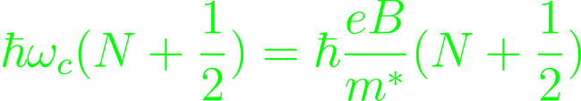
At small magnetic fields, the slope in the horizontal resistivity is only dependent on density, while the vertical resistivity is larger for 2DES with many defects. The quantization of the Hall effect, which is basically just a form of Lorentz-force applied to a valence electron, occurs when the magnetic field is high enough to catch the electron in a closed loop, where it doesn't scatter on defects, and at low temperatures, there are no phonon scatterings either. Then the Drude theory of charge transport doesn't make sense anymore. A different form of quantization has to be employed to square the circle. The magnetic field also quantizes the levels in of the energy spectrum. Previously, the results is characterized through the wave vectors in the x and y direction. Quantizing it with the magnetic field gives potential disks cut from the hollow cone. Intuitively, this comes from the cyclotron frequency that the spinning electrone gets, which takes the place in the usual
This effect also separates the density of space into equidistant packets. These are the "Landau Levels", and they can be partially filled. These partially filled space aren't lost. The degeneracy of Landau levels scales with the magnetic fields:

Introducing disorder will broaden the Landau levels. The electron spin will be visible in the typical Zeeman energy split consisting of the effective g-factor (dependent on material and crystal orientation) and Bohr magneton, multiplied with the magnetic field. The full Hamiltonian should then look like this

The full energy will gain a dependency on location. If the Fermi energy lies on one of the energy eigenvalues, the electron transport occurs as if throughout the entire region of the measured sample. If it doesn't, typically all states are localized. No vertical voltage is measured on the sample and the electron-transport only happens at the edge of the sample, as if in 1-dimension. In these cases, the Drude-model breaks down.
For every filled Landau level, there will be a 1D transport channel at the sample edges. Because of the circular paths of the electrons, the channels are directed in opposite directions, which gives each sample a chirality. In this model, any defects in the channel don't destroy it, so there is no backscattering on defects.
Quantum oscillations can be simulated. Usually, the results of these simulations feature a widening oscillation, where the frequency is damped with increasing magnetic field strength, and the amplitude is damped by increasing temperature. In fact, high enough temperatures may kill the effect entirely. In the case of low effective mass, the oscillations grow relatively rapidly to their maximal amplitude, and then continue their oscillations unimpeded. High effective mass damps all oscillations up to about 1 Tesla, beyond which slow oscillations may build up in low temperature regimes. Typically high effective mass prevents this from happening. In cases of low carrier concentration, the frequency tends to be very low.
The quantum effect of higher temperatures is that several Landau levels are simultaneously partially filled. This gives the Fermi-Dirac distribution a smoother downward slope, as opposed as the "perfect" box. Landau levels can however be spread apart in order to filter electrons down the schema. In theory, this can counteract the effects of elevated temperatures.
Measurement Methods in Various Dimensions
In 2DEGs, the application of an external magnetic field creates a split of energy levels along Zeeman energies. These levels are of course characterized by their spin orientation. This energy gap is called "electron-spin resonance" (ESR) with a Zeeman energy (difference) of

meaning the splitting (and hence excitation frequency) increases linearly with the magnetic field. The measurement of these 2D ESRs happens through the vertical voltage on a Hall-Bar, experiencing excitation through microwave frequency. The electron spin of course contributes to the nuclear spin, which gets its own Zeeman energy. Since spin is not intrinsic, and the electron spin is not constant, the spin state of nuclei fluctuates continuously, which means the hyperfine interaction is also not constant. Hyperfine interaction is interaction between electron- and nuclear spin. The nuclear magnetic moment generates a local field, acting on the electron spin, and the other way around. In quantum dots, this phenomenon can destroy coherence. The Hamiltonian is H = AIS, where A is the probability density of finding the electron at the nucleus.
1D systems are a little difficult to create. The edge channels in the quantum Hall effect are an example of a 1D system. There are also methods to grow or etch/gate 1D systems. Most centrally, the idea is to create a space in which only motion in 1 dimension is possible. The conductivity is independent of the channel length either way, so having a very short, very thin bridge, or gated gap. An effective potential, can be built up in such a gated system using an external voltage. The potential in this case will be that of a harmonic saddle point with discrete energy levels and a 1DEG. From there, the approach is analogous to that of a 2DEG, meaning solving the Schroedinger equation without the presence of a magnetic field, but instead confinement potentials in two spatial axes. The solution includes two of these quantized energy terms.
As per usual, only electrons near the Fermi energy participate in transport, and at low temperatures in quantized systems, they can be assigned a uniform wavelength directly at the Fermi edge. Because the energy eigenstates are shaped like the harmonic oscillators, the Fermi energy intersects with these levels at two points (or none). Each level it intersects with is read as a "subband", which contributes a current of 2e²/h. The steps in the gate voltage at low temperatures and without an external magnetic field might have steps smaller than these quantized steps. This is because of factors impeding the currents, such as Ohmic contacts, scattering/interaction between modes and electron-electron interaction. Changing the voltage applied to the metallic gates can change the number of modes participating in transport. At higher temperatures, the steps in the current are smeared out due to the thermal excitation.

External magnetic fields lift the spin degeneracy and increases the confinement energy. This modifies the effective mass. The energetic splitting of the subbands increase, and steps become much longer.
Quantum dots are 0D systems. Lateral quantum dots can be constructed by having two plunger gates face one another. The quantum dot will be generated in between, in the space left empty. At the plunger gates, the voltages are all negative. The sides of the construction create a weakly permeable barrier in the same way capacitors create permeable barriers. Fermi's Golden Rule provides the transition rate.

The double tunnel the confines electrons that enter the system. The quantum dot is coupled to the environment. The stored capacitive energy can be approached classically

Of course there are discrete energy states in the quantum dot. Adding a single electron to the quantum dot requires a quantized amount of energy

Varying the voltage at the plunger gate creates a pattern reminiscent of the SdH effect, with narrow conductivity peaks separated by values of almost no conductivity. These are called "Coulomb blockade oscillations". Mapping the conductance of the gate against that of the quantum dot creates a pattern in which the atomic transistor can be modeled as "off" and "on" in diamond-shaped areas of the diagram. This is the "Coulomb Diamond". The conductance valleys create blockades in a way that no transport can occur. This means that each dot contains a fixed number of electrons. Quantum dots are analogous to artificial atoms, in their discretized energies with angular momentum degeneracy. The Hund's rules and the shell structure can be correlated to the electron population. Quantum dots can be serialized. In these setups, the mechanics of spin-flips and the Pauli-Principles can be observed on a micro-scale.